Lightwave Electronic Devices
Lightwave electronics, namely electronic processes that are driven directly by the electric field of the optical pulse, enables the generation and control of optical and electronic processes with attosecond precision (see for instance Kruger 2011, and Sansone 2006). Applications include attosecond microscopy and spectroscopy (Luu 2015), PHz signal processing of optical waveforms (Kim 2013), and carrier-envelope phase (CEP) detection and stabilization (Paulus 2001). Over the last several years, we have investigated and engineered solid-state lightwave electronic devices that bring the same optical-field-driven physics of gas-phase lightwave electronic systems to a compact, low-cost solid-state device. Below we summarize our work in this area over the last few years.
On-Chip Carrier-Envelope Phase Detection
At the very end of 2016, we published a comprehensive paper in Nature Physics (Putnam 2016) outlining the development and characterization of an on-chip absolute phase (i.e. CEP) meter for optical pulses. This device utilized an array of nanostructured, plasmonic devices to enhance the optical field and achieve field-dependent, optical-tunneling emission from each nanostructure’s surface (see Fig. 1). Key results of this work include:
- Fabrication and optical characterization of an array of plasmonic devices, with resonances spanning from 950 nm to 1250 nm.
- Demonstration of transition from multiphoton to field-dependent emission using planar device arrays, with freespace electron transport across planar electrodes on the chip.
- Demonstration that the photoemitted current is CEP dependent, and can be used to track the carrier envelope phase in real time.
- Developed analytic resonator + emission model that accurately accounts for plasmonic response and CEP response.
Using similar devices, we are actively studying properties of the CEP response and how it relates to fundamentals of the emission process so that we might engineer improved devices. We also recently demonstrated that autocorrelations performed using optical-field emission from the nanostructures provide information about the precise electromagnetic response of the plasmonic devices in the time-domain.
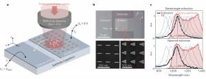
Fig. 1 Absolute phase meter for optical pulses. (a) Device sketch indicating incident optical pulse, the emitter array, and electron trajectories from the emitter pad to the collector pad. The emitter and collector pads are fabricated from indium tin oxide (ITO) to provide a simultaneously conductive and transparent substrate. (b) Scanning electron micrographs of a device array. The top shows the entire pad of an array of devices. The bottom two images show a zoom-in of rod- and triangle-type devices. The tips have a radius of curvature of approximately 5 nm. (c) Optical extinction spectra indicating the plasmonic resonance position for each device type, showing how the device geometry can be used to tune the plasmonic response. The red curve indicates the source spectrum with a transform limit of around 10 fs centered at 1.2 µm.
Multiphoton vs. Optical-Field Electron Emission in Solids
In the last few years we have analyzed the transition from multiphoton to optical-field electron emission in solid-state devices. While this transition has been carefully analyzed in gas-phase systems (Zimmermann 2017), there remain many unresolved aspects of the transition from multiphoton to optical-field emission in solids. For instance, theoretical modeling always indicates that channel-closings should cause strong dips in photoemission yield at particular intensities. However, most studies of photoemission yield from solids show only smooth, featureless curves (see for instance Bormann 2010). In performing a detailed experimental analysis, we found that the photoemission yield curve in silicon does indeed exhibit this structure, along with an enhanced emission yield relative than what is expected in the multiphoton region (see Fig. 2).
Analysis integrating the time-dependent Schrödinger equation (TDSE) with comparison to time-dependent perturbation theory was used to explain all the features of the data using a time-domain picture (Keathley 2017a and 2017b). We found that electrons form standing wave packets inside the oscillating field at the surface, thus enhancing the emission. Due to an AC Stark shift of the potential barrier, eventually the injected electrons lose momentum, and their emission cut off leading to channel closure. The reduced visibility of the channel closures comes from integration over the focal spot, as well as the ground state energy distribution. In fact, the latter was key to seeing the structure in silicon as it has a narrower ground state energy distribution than a typical metal due to the band gap.
Unlike gases, solids provide much greater leverage in controlling the emission process and properties of the emitted electrons, as both the band-structure and geometry of the emitter (and thus the electric field profile) can be engineered. We feel that future measurements of the outgoing momentum distribution will elucidate how properties, such as the effective mass tensor, might also play a role in controlling the spatial distribution of emitted electrons.
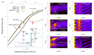
Fig. 2 Transition from multiphoton to optical-field emission from silicon nano tips. (a) Experimental data (green crosses) bends over indicating a transition from multiphoton to optical field emission. The red curves indicate results from integrating the TDSE with and without spatial averaging (solid red and dashed red curves respectively). The black curve is what is predicted by the TDPT. Enhanced emission arises due to coherent electron dynamics at the tip, shown in (b-g). The inset shows the modeled potential with at the tip surface, modulated by a decaying optical field. (b-g) Plots of the square magnitude of the electron wavefunction during emission. The extra kink and drop in emission are due to the electronic wavepackets losing energy due to buildup of the ponderomotive potential at the tip surface.
References
(Bormann 2010) R. Bormann, M. Gulde, A. Weismann, S. V. Yalunin, and C. Ropers, “Tip-Enhanced Strong-Field Photoemission,” Phys. Rev. Lett., vol. 105, no. 14, p. 147601, 2010.
(Keathley 2017a) P. Keathley, W. Putnam, G. Laurent, L. Velasquez-Garcia, and F. Kärtner, “Role of the Ground State in Strong-Field Photoemission Yield from Si Nanotips,” presented at the 6th International Conference on Attosecond Physics, Xi’an, China, July 2017.
(Keathley 2017b) P. D. Keathley, W. P. Putnam, G. Laurent, L. F. Velásquez-García, and F. X. Kärtner, “Examining the Transition from Multiphoton to Optical-Field Photoemission From Silicon Nanostructures,” arXiv:1708.05265 [cond-mat, physics:physics], Aug. 2017.
(Kim 2013) K. T. Kim et al., “Petahertz optical oscilloscope,” Nat Photon, vol. 7, no. 12, pp. 958–962, Dec. 2013.
(Kruger 2011) M. Kruger, M. Schenk, and P. Hommelhoff, “Attosecond control of electrons emitted from a nanoscale metal tip,” Nature, vol. 475, no. 7354, pp. 78–81, Jul. 2011.
(Luu 2015) T. T. Luu, M. Garg, S. Y. Kruchinin, A. Moulet, M. T. Hassan, and E. Goulielmakis, “Extreme ultraviolet high-harmonic spectroscopy of solids,” Nature, vol. 521, no. 7553, pp. 498–502, May 2015.
(Paulus 2001) G. G. Paulus et al., “Absolute-phase phenomena in photoionization with few-cycle laser pulses,” Nature, vol. 414, no. 6860, pp. 182–184, Nov. 2001.
(Putnam 2016) W. P. Putnam, R. G. Hobbs, P. D. Keathley, K. K. Berggren, and F. X. Kärtner, “Optical-field-controlled photoemission from plasmonic nanoparticles,” Nat Phys, vol. 13, pp. 335–339, Dec. 2016.
(Putnam 2017) W. Putnam et al., “Probing the Femtosecond Response of Plasmonic Nanoparticles with Strong-field Photoemission,” in Conference on Lasers and Electro-Optics (2017), paper FM3H.1, 2017, p. FM3H.1.
(Sansone 2006) G. Sansone et al., “Isolated Single-Cycle Attosecond Pulses,” Science, vol. 314, no. 5798, pp. 443–446, Oct. 2006.
(Zimmermann 2017) H. Zimmermann, S. Patchkovskii, M. Ivanov, and U. Eichmann, “Unified Time and Frequency Picture of Ultrafast Atomic Excitation in Strong Laser Fields,” Phys. Rev. Lett., vol. 118, no. 1, p. 013003, Jan. 2017.